Monday, 19 January 2015

Final Year Project 2 (Week 14)

Week 14

Title of activity: Industry day S2’2014

Venue: Gemilang Hall

Time: 8.00am – 12.30pm (FYP 2 Degree Presentation)
·                               8.00am (booth and poster setup)

·         All students of FYP 2 must register first before assessors are coming 9.00am (assess begins)

·         Assessed by Sir Akram Dandu and Dr Nubli

Project Presentation Assessment Criteria:
·         Clarity of the project introduction
·         Clarity of the objectives and achievement of the objectives
·         Clarity of project background and methodology
·         Understanding of results, results analysis/ discussion and conclusion of the project
·         Functionality - rational reasons are given for non-functionality or partially working project with reasonable and acceptable explanation
·         Innovative and Creativity - project design in terms of neatness, creativity, innovative, marketability, sophisticated, futuristic and practical  applications
·         Clarity of explanation and structure of research outcomes / findings / simulation results
·         Understanding of case study, results and data analysis/ discussion and conclusion of the project
·         Originality and preparation of materials
·         Ability to handle questions - able to answer correctly to questions related to the facts, theories and process presented
·         Understanding of project – demonstrate sufficient knowledge gain from the project
·         Interpersonal skills

Final Year Project 2 (Week 13)

Week 13

Title of activity:

  • Create a poster

Description:


     1.    Create a poster by using Microsoft Word version 2013
     2.    Size of poster required is A1 measurement
     3.    The figure below shows the poster that I have done.

Outcome:


Final Year Project 2 (Week 12)

Week 12

Title of activity:

  • Make list of poster requirements

Description:

Before making a poster, I have seen some examples of posters available at FYP room to get the idea. Most of the posters in the room belong to students who have taken the course of FYP.

Procedure:

The poster will include some of these requirements with explanation

            ·         Project Title
            ·         Student’s name
            ·         University
            ·         Supervisor’s name
            ·         Abstract  
            ·     Objectives
            ·         Methodology
            ·         Diagram
            ·         Results
                Conclusion


Final Year Project 2 (Week 11)

Week 11

Title of activity:

  • Do selection of the program

Procedure:
     
     1.    Design the program using PICC compiler software

     2.    Do selection for the program is important because the program is the main process for         the project. For this project, PICC compiler was selected because the program is simple       and easy to understand.

     3.    Steps to write down the program:
  •        Open PICC compiler shortcut
  •     Open new file
  •     Save as new file. The new file that we save (example : HAZIQ) will have extension c             (example : HAZIQ.c)
  •       Write down the program

      Outcome:


Final Year Project 2 (Week 10)

Week 10

Title of activity:

  • Apply the components on copper board and do the soldering process


Procedure:

  1.    To solder the components on the board according to the PCB design for each circuit.
       2.    To make a connection for all component on the copper board.
       3.    Soldering components on PIC circuit (Figure 1)
       4.    Soldering components on Relay circuit (Figure 2)
       5.    Top view: PIC circuit (Figure 3)
       6.    Bottom view: PIC circuit (Figure 4)
       7.    Top view: Relay circuit (Figure 5)
       8.    Bottom view: Relay circuit (Figure 6)
    
    
    Outcome:


Conclusion:

After soldering the entire component on the copper board. The circuit must be troubleshoot to check whether the components are connected properly according to the PCB layout.


Friday, 16 January 2015

Final Year Project 2 (Week 9)

Week 9

Tittle of activity:

Make a drilling process after etching the circuit design.

Description:

Holes through a PCB are typically drilled with small-diameter drill bits made of solid coated tungsten carbide. Coated tungsten carbide is recommended since many board materials are very abrasive and drilling must be high RPM and high feed to be cost effective. Drill bits must also remain sharp so as not to mar or tear the traces. Drilling with high-speed-steel is simply not feasible since the drill bits will dull quickly and thus tear the copper and ruin the boards.

Procedure:
  1.  In this project, I am using the Pro’s Kit super mini drill 12V to make the drilling process (Figure 1).
  2. Next, drill the holes using a driller (Figure 2).
  3. This is the result after the board had been rubbed by sandpaper to remove the remaining copper that not been covered by carbon ink. Lastly, this circuit is ready to be constructed with the components (Figure 3).

      Outcome:


Final Year Project 2 (Week 8)

Week 8

Title of activity:

Etching process on the copper board according to the PCB layout

Procedure:

  1. Clothes iron will be used to iron the PCB design to attach on the surface of copper board (Figure 1).
  2. After attaching the PCB design on to the copper board. It will be placed into the etching acid. This process takes about 20 minutes to remove the remaining copper that is not needed (Figure 2).
  3. The results of the etching process. Copper is not needed will be eroded, only copper that covered by carbon ink will remain on the board and form a circuit (Figure 3).
      Outcome:


Final Year Project 2 (Week 7)

Week 7

Titles of activity:
-          
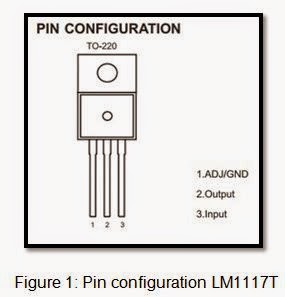
  •       Research and findings (LM 1117T – Voltage Regulator)

                             
      Analysis:

  • The LM 1117 is a series of low dropout voltage regulators which can provide up to 1A of output current. The LM1117 is available in four fixed voltage, 1.2V, 1.8V, 3.3V and 5.0V. Additionally it is also available in adjustable version. On chip precision trimming adjusts the reference/ output voltage to within 2%. Current limit is also  trimmed to ensure specified output current and controlled short-circuit current. The LM1117 series output current and controlled short-circuit current. The LM1117 series is available in SOT-233 and TO-220 packages. A minimum of 10uF tantalum capacitor is required at the ouput to improve the transient response and stability.  


     FEATURES:
  1.      Adjustable and Fixed of 1.2V, 1.8V, 3.3V, 5.0V
  2.          Space saving SMD types of SOT-223
  3.          1.2V Drop-out Voltage
  4.          1.0A Output Current
  5.          Line Regulation Typically
  6.          Current Limiting and Thermal Protection


APPLICATION:

  1.          Post regulator for switching DC/DC switching
  2.          High Efficiency Line Regulator
  3.          Battery Charges
  4.          PC Add on Card
  5.          Motherboard clock supplies
  6.          LCD Monitor
  7.          Set-top Box 


Final Year Project 2 (Week 6)

Week 6

Tittles of activity:
Research about the Relay 5Vdc (Single Pole Double Throw)

Analysis:

Relay is an electromagnetic device which is used to isolate two circuits electrically and connect them magnetically. They are very useful devices and allow one circuit to switch another one while they are completely separate. They are often used to interface an electronic circuit (working at a low voltage) to an electrical circuit which works at very high voltage. For example, a relay can make a 5V DC battery circuit to switch a 230V AC mains circuit. Thus a small sensor circuit can drive, say, a fan or an electric bulb.

A relay switch can be divided into two parts: input and output. The input section has a coil which generates magnetic field when a small voltage from an electronic circuit is applied to it. This voltage is called the operating voltage. Commonly used relays are available in different configuration of operating voltages like 6V, 9V, 12V, 24V etc. The output section consists of contactors which connect or disconnect mechanically. In a basic relay there are three contactors: normally open (NO), normally closed (NC) and common (COM). At no input state, the COM is connected to NC. When the operating voltage is applied the relay coil gets energized and the COM changes contact to NO. 

Outcome:

Figure 1 below shown a Relay and its symbol:


Table 1 below shown a Pin Description of a Relay:


  • There are 5 Pins in a relay. Two pins A and B are two ends of a coil that are kept inside the relay. The coil is wound on a small rod that gets magnetized whenever current passes through it


  •  COM/POLE is always connected to NC (Normally connected) pin. As current is passed through the coil A, B, the pole gets connected to NO (Normally Open) pin of the relay.


Conclusion:

From this week activity, we can conclude that a relay is an electrically operated switch. Current flowing through the coil of the relay creates a magnetic field which attracts a lever and changes the switch contacts. The coil current can be on or off so relays have two switch positions and they are double throw (changeover) switches


Final Year Project 2 (Week 5)

Week 5


Tittles of activity:
  • Research about the 'Bluetooth Module' HC-05
Analysis:
  • Bluetooth serial module is used for converting serial port to Bluetooth. These modules have two modes: master and slaver device. The device named after even number is defined to be master or slaver when out of factory and can’t be changed to the other mode. But for the device named after odd number, users can set the work mode (master or slaver) of the device by AT commands.
  • When HC-05 is out of factory, one part of parameters is set for activating the device. The work mode is not set, since user can set the mode of HC-05 as they want. The main function of Bluetooth serial module is replacing the serial port line, such as:

1.  There are two MCUs want to communicate with each other. One connects to Bluetooth master device while the other one connects to slave device. Their connection can be built once the pair is made. This Bluetooth connection is equivalently liked to a serial port line connection including RXD, TXD signals and they can use the Bluetooth serial module to communicate with each other.

2.    When MCU has Bluetooth slave module, it can communicate with Bluetooth adapter of computers and smart phones. Then there is a virtual communicable serial port line between MCU and computer or smart phone.

3.  The Bluetooth devices in the market mostly are slave devices, such as Bluetooth printer, Bluetooth GPS. So, we can use master module to make pair and communicate with them. Bluetooth Serial module’s operation doesn’t need drive, and can communicate with the other Bluetooth device which has the serial. 

Bluetooth Module HC-05


Wednesday, 14 January 2015

Final Year Project 2 (Week 4)

Week 4

Title of project:
  • Re-design flow chart exactly with the project that developed


Description:

  • The flow chart that made is based on existing flow chart in the previous post for FYP 1 and for the other thing is according to the project that are being implemented. The result that obtained is such the project outcome below.


Final Year Project 2 (Week 3)

Week 3

Title of project:
  • Re-design block diagram exactly with the project that developed


Description:
  • A block diagram become one of the important part in develop a project.  The block diagram need to re-designed because some of the component that listed in FYP 1 was changed with the other component. The changes that made is for the purposes to reduce project costing and also to make the project more efficient and easy to used.


Outcome:


Final Year Project 2 (Week 2)

Week 2

Tittles of activity:

  •  Estimate all components that has been used to develop a project for FYP 2

Objective:

  • The main purpose is to ensure that component is correct and suitable to develop a project.
  • To develop a project with an economical and low cost budget in terms a pricing.
  • To avoid the loss during buying the components if the components not suitable to develop the project.

Outcome:

  • Table 1 and table 2 below shown the all components that have been used to develop a project for FYP 2. This project is divided into two parts which is hardware development and software development.

Hardware Development:


Software development:


Conclusion:


  • For this week activity, all components to develop a project for FYP 2 are estimated. For the next step, research all the components above to know their features, function and so on before installation the components on the project.


Final Year Project 2 (Week 1)

Week 1


Tittles of activity:

  • Discussion with project supervisor
  •  Project scheduling


Objective:
  •           To update any related matter  that has been made for FYP 2 to the project supervisor
  •           To manage weekly activities that will be made systematically
  •           To ensure all task that should be made completed on time


Procedure:
  • The main objective of this discussion is to update any progress that has been made for FYP 2 to the project supervisor. Simply, the content in discussion is about the FYP 2 assessment that should be made in term of the due date for submission, report formats and report content. Besides that, to fulfill subject requirement according to date line that given, a gantt will be created to make it as a guidelines and to ensure all task completed on time.

Result:
  • The outcome this activity is such as the figure 1 below:


Conclusion:


  • All tasks that related with the FYP 2 will be referred on that gantt chart until at the end of the date line for FYP 2. For the next progress report, the topic that will discussed is specific about the project research that made for FYP 2.